Metallic Glasses
Amorphous metals, also known as metallic glasses differ from conventional metals in that they lack crystalline structure. The atoms in the amorphous structure are randomly arranged, like in a liquid, rather than sitting on a repeatable, orderly lattice. This lack of crystalline structure means that metallic glasses also lack crystalline defects, such as grain boundaries and dislocations. Without these "weak spots", metallic glasses exhibit extraordinary mechanical properties, magnetic behavior, and corrosion resistance.
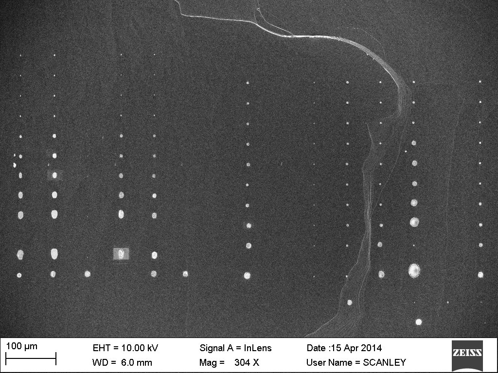
Zinc Oxide Nanowires
The ConnSCU-CNT at SCSU has worked to characterize Zinc Oxide (ZnO) nanowires and nanowire substrates fabricated by the Osuji Lab at Yale. The long range goal of the project is the production of low cost – high efficiency solar cells. ZnO nanowires will be the electron conductors in these cells. In order to effectively capture and conduct the electrons, the nanowires need to be grown as trees in a forest; tall, narrow, growing vertically and evenly spaced. The work at SCSU involves characterization of ZnO nanowire samples using Scanning Electron Microscopy (SEM). Analysis of SEM images can be used to characterize the height, diameter and uniformity of growth in order to assist with refining the conditions and procedures used to fabricate the nanowires. Top Left: close-up of nanowires viewed from the top down. Top Right: low magnification view of nanowire forest viewed from the top down.
Dip Pen Nanolithography
Dip pen nanolithography is a direct write, tip based lithography technique capable of multi-component deposition of a wide range of materials at the nano-scale. Parallel arrays of atomic force microscope tips allows for simultaneous patterning of multiple materials on a substrate. A piezoelectrically controlled tray contains a chip of etched micro-channels that serve as inkwells and a substrate for deposition. The tips are dipped into separate ink-channels and then the solution may be deposited onto a substrate in a pre-determined pattern with as low as single digit nanometer precision. Modulating the level of humidity in the vessel, temperature, and dwell time affects the size of the nanoparticle patterns. A NanoInk NLP 2000 will be used to pattern different catalytic nanoparticle solutions simultaneously in order to determine an efficient process for synthesizing aligned carbon nanotubes (CNTs) on a substrate using chemical vapor deposition (CVD). By patterning different nanoparticle solutions next to each other, identical growth conditions may be compared for different catalysts in a streamlined analysis process. Fe, Co, and Ni nanoparticle solutions will be patterned on silicon, mica, and sapphire substrates using acetylene or toluene as the carbon source for CNT synthesis.
Carbon Nanotubes
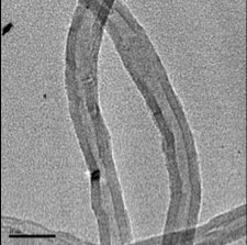
Projects on synthesis of carbon nanotubes are ongoing at the Center. In the figure to the left, a Nanotech SSP-354 Chemical Vapor Deposition Furnace was used to synthesize multi-walled carbon nanotubes. A liquid phase precursor (hydrocarbon with nanoparticle catalyst mix) was injected into the tube furnace with a flowing carrier gas. Carbon nanotubes were grown in high purity and collected on the surface of the quartz tube. The furnace temperature was varied during synthesis resulting in changes in carbon nanotube inner and outer diameters and in total production of carbon nanotubes.
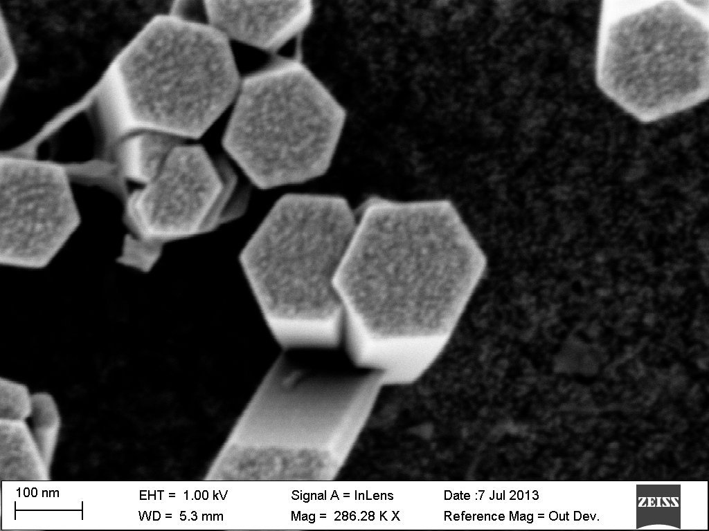
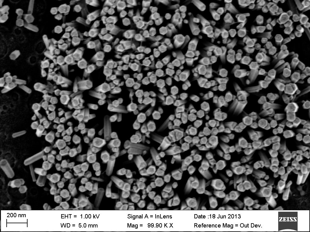
Silver Nanoprisms
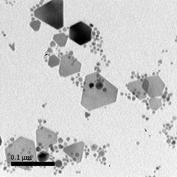
Colloidal silver nanoprisms can be synthesized in a number of ways. The most common technique is a photochemical reaction using silver nanoparticles in a citrate and bis(p-sulfonatophenyl)phenylphosphine dipotassium solution. Alternatively, silver nanoprisms can be synthesized using a thermal, chemical reduction method in which capping agents encourage preferential growth on specific crystalline facets (specifically the {111} facet). In this study, silver nanoprisms were grown by both methods and analyzed with transmission electron microscopy and UV-Vis-NIR spectroscopy.